Acceleration Direction
On SDI’s surface mount chips and 1-axis modules, the sensitive axis is perpendicular to the bottom of the package. The marked side with the model information is considered the front of the accelerometer.
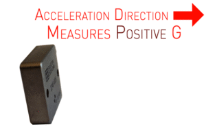
SDI marks the “X,” “Y,” and “Z” axes on its triaxial accelerometers. The model above can be applied to each axis.
Bias
The accelerometer output with no acceleration present. For our differential output analog accelerometers, it is a signed quantity that is expressed in terms of either g or output volts and is ideally equal to zero g or zero volts.
Bias Calibration Error
Expressed as a percentage of span. For example, a 2% of g-span error for a 5 g full scale device would equate to +/-2% of 10g = +/-0.2g. This +/-2% error in terms of output voltage for a 5g analog accelerometer would be +/-.02 x 8V or +/-160 mV. This same 2% error in terms of output frequency for a 5g digital accelerometer operating with a 250 kHz clock would be +/-.02 x 250 kHz = +/-5 kHz.
Bias Temperature Shift
Expressed as ppm of span per deg C. For example, the percent of span bias shift that would occur for a 25g full scale device with a +/-200 ppm of span per deg C rating and a 55 deg C rise from room temperature would be: +/-200 / 1,000,000 x (80C – 25C) x 100% of span = +/-1.1% of span. The g shift would be +/-1.1% of 50g = 0.55 g. This error in terms of output voltage for a 25 g analog accelerometer would be +/-1.1% of span = +/-1.1% of 8 V = 88 mV. This same error in terms of output frequency for a 25 g digital accelerometer operating with a 250 kHz clock would be +/-1.1% of span = +/-1.1% of 250 kHz = +/-2.75 kHz.
Cross Axis Sensitivity
A percentage of the level of applied acceleration in a direction that is 90 degrees to the accelerometer’s sensitive axis. If, for example, a 5g acceleration is applied at 90 degrees to the sensitive axis, the output would measure no greater than 3% of 5g or 0.15g. The majority of cross axis error stems from the sense element structure not being perfectly parallel to the bottom of the LCC package. This happens due to the lack of perfect parallelism from three sources; the LCC case’s cavity floor vs its bottom surface, the sense element die’s bottom surface vs the LCC case’s cavity floor separated by an epoxy layer, and the sense element die’s top & bottom surface finish.
We only measure cross axis sensitivity during qualification testing but it is controlled by the specification drawings for the piece parts that go into making the accelerometer. The ceramic substrate drawing specifies a 1 microinch Ra surface finish. The LCC package drawing specifies .002″ flatness for the die attach surface and .003″ flatness for the bottom surface. The die attach epoxy adhesive used to secure the sense element die to the LCC package cavity contains 2% glass spacer beads. Each die is pressed towards the cavity surface so that the die seats on the beads which provides a reliable .0029″ thick bond line.
Full Scale
The accelerometer’s range of output from 0g to the maximum G rating of the device. This can be discussed in G’s or in output signal. In G’s, that would be 0 to 100G for a 100G device. SDI’s accelerometers support both differential and single ended outputs. For an accelerometer with a +/-4 VDC output in differential mode that would be 4000 mV, and in single ended mode would be 2000 mV.
G
A unit of acceleration equal to the standard value of the Earth’s gravity. 1g = 9.8085 m/s2 or 32.180 ft/s2.
General Accuracy
Determined by you for the operational range you intend to use the device over. Each error source’s contribution must be taken into account. The errors can then be summed up but this may yield a pessimistic view of the overall error because these individual errors are non-correlated (one does not affect the other). Alternatively, you can calculate the total error as the square root of the sum of the squares of all the error sources.
Non-Linearity
A percentage of span and is the deviation of the accelerometer output from its least-squares-fit scale factor (sensitivity) line slope. Measurements are limited to -90% to +90% of full scale or from -65g to +65g, whichever range is smaller.
PSSR
Power Supply Rejection Ratio: A measure of the variation in the accelerometer’s bias shifts as its power supply voltage is varied.
Scale Factor
The ratio of the change in output to a unit change in the input acceleration. Since the output of most accelerometers is slightly non-linear, the scale factor value is defined as the slope of the least-squares-fit line to the acceleration input vs output curve. Our measurements are limited to -90% to +90% of full scale or from -65g to +65g, whichever range is smaller. For our analog output accelerometers, the units for scale factor are in millivolts per g (mV/g). For digital output accelerometers, the units for scale factor are in counts per g. We measure the output at 33 total points, 16 between 0 and +90% of full scale, 16 between 0 and -90% of full scale and at 0g. The Scale factor is the slope of the least squares fit line for these 33 points.
Scale Factor Error
The percentage difference between the slope of a least squares fit line to the measured (actual) scale factor curve and the slope of the ideal scale factor line. A +/-2% error for a 50g full scale analog accelerometer would be +/-2% of 8V/100g = +/-2% of 800 mV/g = +/-16 mV/g. A +/-2% error for a 5g digital accelerometer operating with a 250 kHz clock would be +/-2% of (250 kHz)/10 g = +/-2% of 25 kHz/g = +/-500 Hz/g.
Scale Factor Temperature Shift
Expressed as ppm per deg C. For example, the percent shift in scale factor that would occur for a device with a +300 ppm per deg C rating and a 60 deg C rise from room temperature would be: +300 / 1,000,000 x (85C – 25C) x 100% = +1.8%. For an analog 10g device, the scale factor would rise from its nominal (8 V)/(20 g) = 400 mV/g at +25C to 400 mV/g +1.8% = 407.2 mV/g. For a digital 10g device operating with a 250 kHz clock, the scale factor would rise from its nominal (250 KHz)/(20 g) = 12.5 kHz/g at +25C to 12.5 kHz/g + 1.8% = 12.725 kHz/g.
Sensitivity
Sensitivity is a function of the G level and full scale output. Take the accelerometer output range, for example 4V (which is SDI’s normal differential output), and calculate its equivalent value in mV. For purposes of this example, that equals 4000 mV. Divide that mV number by a sensor’s g range, let’s say ±50 g, so 4000/50 = 80 mV. This means that ±1 g of acceleration is equivalent to approximately 80 mV of output. Single ended output is half of differential, so sensitivity is also half.
Span
The magnitude of the overall measurement range of the accelerometer from its minus full scale to plus full scale. For example, our 5g full scale accelerometers have a 10g input span (from -5 to +5g). The span can also be expressed in terms of the output where the Sensitivity (or Scale Factor) of the device is used to convert between input span and output span. A 5g analog accelerometer has an output voltage span of 800 mV/g x 10g or 8000 mV. A 5g digital accelerometer has an output span of 25 kHz/g x 10g or 250 kHz (assuming a 250 kHz clock is being applied).
Thermal Transient Error
Occurs when a drastic change in operating temperature results in a larger change in output than would be predicted by the device’s bias and scale factor temperature coefficients. Piezoelectric type accelerometers are subject to this error because piezoelectric crystals develop a voltage across them if the temperature change rate is within its bandwidth. Silicon Design’s MEMS DC accelerometers are insensitive to this type of error because of their variable capacitive design and see at most a .1% of span change during drastic thermal changes.